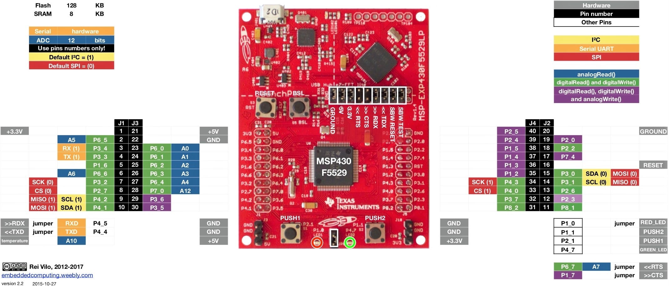
MSP430F5529LP?
Texas Instruments’ Launchpad Microcontrollers are used in UOE Racing’s electric car projects. UOE’s entry for the Shell Eco-Marathon competition relies on an MSP430 Launchpad board to control a DRV8323, which controls a brushless DC (BLDC) motor. As part of a small team, I am responsible for improving the code to control the DRV8323, and by extension, the BLDC.
A timer, the CPU peripheral that ticks down to zero then interrupts the CPU,
is a very practical tool for embedded development. This is a short guide,
written with the intent of being a self-reference, on how to configure the
timer within the MSP430F5529 MCU.
When working with TI Launchpad boards, either the Energia or Code Composer Studio (CCS) IDEs can be used. Energia, an adapted Arduino IDE, is easier for beginners, but lacks the advanced debugging capabilities of CCS. I will be working with both in this document, so please be aware as not all code will run in both environments.
Regardless of the environment, you’ll need the correct headers at the top of your C file or Energia script in order to poke registers and configure peripherals within the MSP430:
#include "msp430f5529.h"
The primary reference for this article is TI’s thousand-page tome 1 with everything you’d ever need to know about the microcontroller.
The Timer_A Peripheral
Timer_A is a timer (who would have guessed?) module with seven capture/compare
registers, CCR0 through to CCR6. The MCU also has B and D timers, but
I suppose I’ll look into those when I run out of channels on Timer0_A5 (there
are two other Timer_A modules on the board!) This timer module
is 16 bits and has up to six channels.
Below is the block diagram from page 462 of TI’s user guide1.

This diagram shows the Timer Block, the top level component of the peripheral,
and the content of each timer channel, labeled with CCRn. Diagrams like this
are useful for understanding what registers can be used to configure the timer.
For instance, in the Timer Block, two dividers ID and IDEX exist between
the 16-bit timer register TAxR and the clock source, allowing us to slow down
time and only tick every x seconds. The clock source itself can be configured
with TASSEL. We need to do some more reading to understand where these can
be configured.
For starters, here are the bits for the Timer_A control register, TAxCTL.
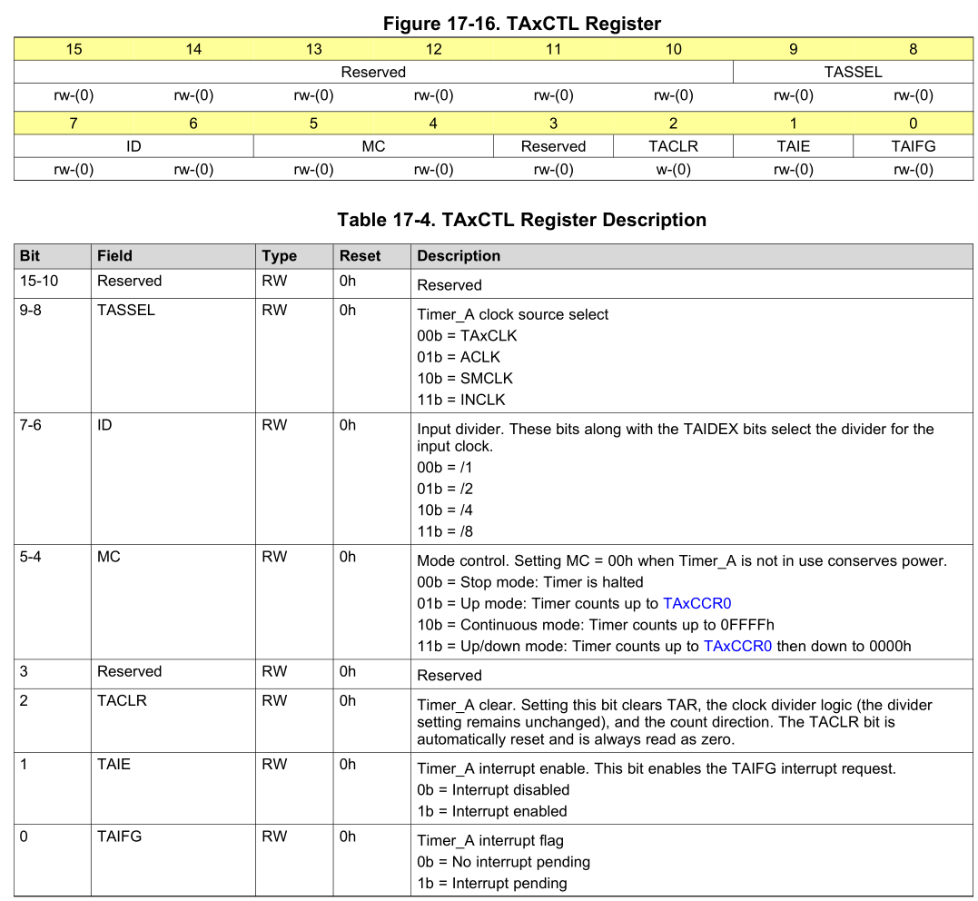
This table tells us everything we need to know about configuring our timer
module! We will refer back to this table when we begin writing code. Note the
configuration bits for previously discussed TASSEL, ID.
Each timer channel also has a configuration register.
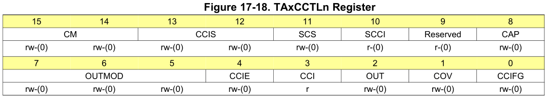
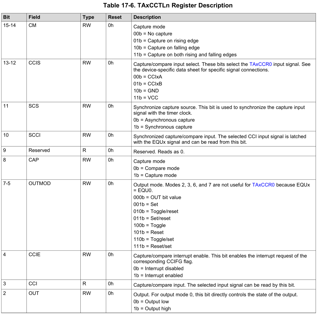
These configuration options are a little more complex. What you need to know for
now is that timer channels can operate in two modes: capture or compare.
The input-capture mode allows us to listen for incoming signals and save the
time of capture to the channel’s TAxCCRn register. Output-compare will trigger
an interrupt when the value stored in TAxCCRn matches the timer value stored
in TAxR.
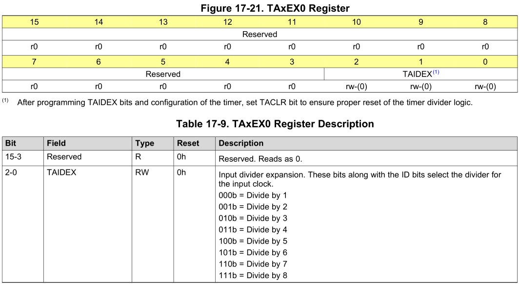
Additionally, we can multiply the prescaler (called input divider in the
diagrams) by an additional, larger number using the TAxEX0 register. For
instance, setting ID0 and IDEX0 to 8 makes the prescaler value 64.
One silly thing to note: when looking at your timer modules in CCS, you’ll
notice you have many, named with the convention TimerX_AY. Here, X denotes
the timer module, and Y denotes the number of channels2.
By reading the manual and tables above, we can conclude that
Timer0_A5 can be configured with the following registers:
The main timer count is stored in
TA0R.Each of the seven timer channels has a control register
TA0CCTLn.The timer is controlled with the
TA0CTLregister.- Bits 9 and 8 control
TASSEL, which should usually be set to10to read from theSMCLK, the sub-main clock. - Bits 7 and 6 control
ID, the prescaler, which divides the input clock by 2 to the power of (the value ofID). - Bit 2 controls
TACLR, which if set to 1, clears the module. - Bit 1 controls
TAIE, which enables theTAIFGinterrupt when the timer overflows. - Bit 0 controls
TAIFG, which is set to 1 when there is an interrupt pending.
- Bits 9 and 8 control
Each channel is controlled by a
TA0CCTLnregister.- Bit 4 is
CCIE, enabling interrupts.
- Bit 4 is
For output-compare, we set a value in
TA0CCRn
A Practical Example
The only registers we need to configure Timer_A are TA0CTL, and for each
timer channel, TA0CCTLn and TA0CCRn. The register TA0R stores the actual
value of the timer. For example, a simple blink program in C would look like the
following:
(Compiled with CCS, 2020-01-12, on an MSP430F5529LP)
#include "msp430f5529.h"

void main(void)
{
    WDTCTL = WDTPW | WDTHOLD;

    P4DIR |= BIT7;
    P4OUT &= ~BIT7;

    TA0CTL = TASSEL_2 + MC_2 + TACLR + ID_3;
    TA0EX0 = TAIDEX_1;

    TA0CCTL1 = CCIE;
    TA0CCR1 = 0xFFFF;

    _BIS_SR(LPM3_bits + GIE);
}

#pragma vector=TIMER0_A0_VECTOR
__interrupt void TIMER0_A0_ISR(void){}

#pragma vector=TIMER0_A1_VECTOR
__interrupt void TIMER0_A1_ISR(void)
{
    P1OUT ^= 0x01;
    switch (__even_in_range(TA0IV, TA0IV_TAIFG))
    {
    case TA0IV_TACCR1:
        P4OUT ^= BIT7; // Toggle the LED bit.
        break;
    default:
        __never_executed();
    }
}
Wow, that’s really difficult to understand! All this program does is toggle an LED every second. Let’s break it down.
Firstly, I’m using a lot of macros, definitions, and TI compiler-specific
pieces of code. Macro expansions like MC_2 set the mode to Timer A mode
control: 2 - Continuous up without specifying the exact bits that need to be
changed. These macros and definitions can all be found in msp430f5529.h.
Viewing the active registers in CCS, we can see the following:
Timer0_A5:
Register:   Value:
  TA0CTL    0x02E1 Timer0_A5 Control [Memory Mapped]
    TASSEL  10 - TASSEL_2  Timer A clock source select
    ID      11 - ID_3  Timer A clock input divider
    MC      10 - MC_2  Timer A mode control
    TACLR   0  Timer A counter clear
    TAIE    0  Timer A counter interrupt enable
    TAIFG   1  Timer A counter interrupt flag
TA0CTL holds the hex value 0x02E1. If we wanted to, we could go ahead and
replace the line setting TA0CTL with this value, but it would be more
difficult to understand. This aside, we can see that the following bits have
been set correctly:
- The
TASSELis set to source 2, theSMCLK. - The
IDis set to 3 which prescales theSMCLKby 8. - The
MCis set to 2, which is continuous mode.
All of the registers on the MSP430F5529LP MCU can be inspected in this manner within Code Composer Studio.
Timer Calculations for 1s blink:

2^16 = 65536 max ticks
~1MHz clock /8 = 125000 Hz
* 65536 ticks = ~1.9 Hz blinks
+ external prescaler /2 => ~1 Hz blinks.
Success!
Here’s a copy of the code with comments:
#include "msp430f5529.h"

/**
 * Timer experiments.
 * Adapted by Ryan Fleck - [email protected]
 *
 * Blinks LED2 at P4.7
 */

void main(void)
{

    // Stop watch-dog timer
    WDTCTL = WDTPW | WDTHOLD;

    // Set the seventh bit of the P4 Data Direction Register to HIGH
    // This allows us to use P4.7 LED as an OUTPUT.
    P4DIR |= BIT7;
    P4OUT &= ~BIT7; // Turns LED off.

    // Configure Timer A0.
    TA0CTL = TASSEL_2 + MC_2 + TACLR + ID_3;
    // From TI example ta0_02:
    // - SMCLK set as clock.
    // - MC - mode control - timer counts up to FFFF and resets.
    // - Clears TAR, previous count, clock divider.
    // - Sets prescaler to 8.

    TA0EX0 = TAIDEX_1;
    // - Sets external prescaler to 2, total of 16

    // Configure Timer A0 Channel 0:
    //TA0CCR0 = 0xFFFF;

    // For counting, we want output-compare mode.

    // Configure Timer A0 Channel 1:
    TA0CCTL1 = CCIE;
    TA0CCR1 = 0xFFFF;

    TA0CCTL2 = CCIE;
    TA0CCR2 = 0xFFFA;

    // Wait for timer interrupts.
    _BIS_SR(LPM3_bits + GIE);

}

/* TimerA has two interrupt vectors:
 *  - One dedicated to CCR0
 *  - One shared by TAIFG, plus all other channels.
 *  - A case statement is used to check which channel
 *    the interrupt was issued from for ch. 1-4.
 */

#pragma vector=TIMER0_A0_VECTOR
__interrupt void TIMER0_A0_ISR(void)
{
    // Handle CCR0 interrupts.
}

#pragma vector=TIMER0_A1_VECTOR
__interrupt void TIMER0_A1_ISR(void)
{
    P1OUT ^= 0x01; // Toggle P1.0
    switch (__even_in_range(TA0IV, TA0IV_TAIFG))
    {
    case TA0IV_NONE:
        break;
    case TA0IV_TACCR1:
        P4OUT ^= BIT7; // Toggle the LED bit.
        break;
    case TA0IV_TACCR2:
        break;
    case TA0IV_TACCR3:
        break;
    case TA0IV_TACCR4:
        break;
    default:
        __never_executed();
    }
}
__even_in_range() allows the compiler to generate more efficient code for the
switch, equivalent to switch(TA0IV)3
Now that we’ve discussed output-compare mode, let’s take a look at input-capture.
To be continued.
TI MSP430x5xx Family User’s Guide, Revision Q, slau208q.pdf , Copyright © 2008-2018 Texas Instruments Incorporated ↩︎ ↩︎
TI MSP430x5xx Timer Training, MSP430m06_TIMERS.pdf , Copyright © 2008-2018 Texas Instruments Incorporated ↩︎
TI Forums: “What does the ‘__even_in_range’ function do?”, link ↩︎